Modified Harvard Architecture: One of the ways by which the number of clock cycles required for the memory access can be reduced is to use more than one bus for both address and data. In the modified Harvard Architecture, One set of buses is used to access a memory that has both program and data, and another that has data alone. Data can also be transferred from one memory to another.
Digital Signal Processors, by B. Venkataramani
Join EEE Made Easy Whatsapp Channel
In the Harvard architecture shown in Fig. there are two separate buses for the program and data memory. Hence, the content of program memory and data memory can be accessed in parallel. The instruction code can be fed from the program memory to the control unit while the operand is fed to the processing unit from the data memory.
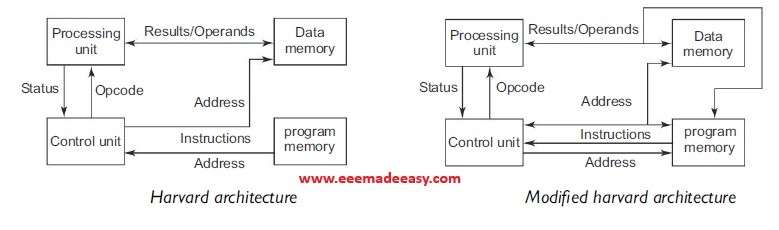
The processing unit, consisting of the registers and processing elements such as MAC units, multiplier, ALU, shifter, etc., are also referred to as the data path.
Join EEE Made Easy Telegram channel
Modified Harvard Architecture
The P-DSPs follow the modified Harvard architecture shown in the above Fig.
One set of buses is used to access a memory that has both program and data, and another that has data alone. Data can also be transferred from one memory to another.
The modified Harvard architecture is used in several P-DSPs, for example, P-DSPs from Texas Instruments and Analog Devices.
With the Harvard architecture, the number of memory accesses/clock cycle was shown to be two.
This can be increased further by using a larger number of buses.
For example, by using three separate address and data buses, the number of memory accesses/clock cycle can be increased to three.
Motorola DSP5600X, DSP96002, etc. have three separate buses. TMS320C54X has four address buses.
Since the cost of an IC increases with the number of pins in the IC, extending a number of buses outside
the chip would unduly increase the price.
Hence, the P-DSP’s use multiple buses only for connecting the on-chip memory to the control unit and data path. For accessing off-chip memory, only a single bus is used for accessing both the program memory and data memory. Because of this, any operation that involves an off-chip memory is slow compared to that using the on-chip memory.
Read also: TMS320C5X Architecture
Book for Digital Signal Processor
Digital Signal Processors, by B. Venkataramani
Join EEE Made Easy Whatsapp Channel
Download EEE Made Easy Ebook PDF Free
Latest Posts in EEE Made Easy
- Energy Efficient Lamps|CFL, LED lamps
 Energy Efficient Lamps: CFL (Compact Fluorescent lamp ) and LED (light emitting diodes) lamp are Energy Efficient Lamps. Energy Efficient … Read more
 - [New] AE KWA Kerala PSC 2026AE KWA Kerala PSC 2026: DETAILED SYLLABUS FOR SELECTION TO THE POST OF ASSISTANT ENGINEER IN KERALA WATER AUTHOERITY AE … Read more
- [New] Electricity Worker KSEB Syllabus 2026|021/2026 Syllabus Kerala PSCElectricity Worker KSEB Syllabus 2026- 021/2026 Syllabus Kerala PSC: DETAILED SYLLABUS FOR THE POST OF ELECTRICITY WORKER IN KERALASTATE ELECTRICITY … Read more
- [Latest]KWA Operator Syllabus 2026|734,735/2025 Kerala PSC syllabusKWA Operator Syllabus 2026 – 734,735/2025 Kerala PSC syllabus: KERALA PUBLIC SERVICE COMMISSIONDETAILED SYLLABUS FOR THE POST OF OPERATOR (DIRECT) … Read more
- [New]Inspector of Legal Metrology Syllabus|613/2025 Kerala PSC SyllabusInspector of Legal Metrology Syllabus– 613/2025 Kerala PSC Syllabus: DETAILED SYLLABUS FOR THE POST OF INSPECTOR OF LEGAL METROLOGY IN … Read more
- [PDF]IE Rules|Indian Electricity Rules 1956IE Rules:The Indian Electricity Rules 1956 was made under section 37 of the Indian Electricity Act, 1910 and redefined after … Read more
- [Latest]Syllabus Sub Engineer LSGD Electricity Wing Thrissur Corporation| 770/2025 Syllabus Kerala PSCSyllabus Sub Engineer LSGD Electricity Wing Thrissur Corporation: DETAILED SYLLABUS FOR THE POST OF SUB ENGINEER IN LSGD(ELECTRICITY WING OF … Read more