8051 Microcontroller Instruction Set : In this post, 8051 Microcontroller Instructions sets are explained with Examples.1.Data transfer instructions,2. Arithmetic instructions,3.Logical instructions,4.Branch instructions,5.Subroutine instructions, and 6. Bit manipulation instructions.
Read also : Addressing modes of 8051 Microcontroller|8051 Addressing Modes
Instruction Timings
The 8051 internal operations and external read/write operations are controlled by the oscillator
clock.
T-state, Machine cycle, and Instruction cycle
T-state, Machine cycle and Instruction cycle are terms used in instruction timings.
T-state is defined as one subdivision of the operation performed in one clock period. The terms ‘Tstate’ and ‘clock period’ are often used synonymously.
The machine cycle is defined as 12 oscillator periods. A machine cycle consists of six states and each state lasts for two oscillator periods.
An instruction takes one to four machine cycles to execute an instruction.
The instruction cycle is defined as the time required for completing the execution of an
instruction.
The 8051 instruction cycle consists of one to four machine cycles.
Eg. If 8051 microcontroller is operated with 12 MHz oscillator, find the execution time for the following four instructions.
- ADD A, 45H
- SUBB A, #55H
- MOV DPTR, #2000H
- MUL AB
Since the oscillator frequency is 12 MHz, the clock period is, Clock period = 1/12 MHz = 0.08333 µS. Time for 1 machine cycle = 0.08333 µS x 12 =1 µS.
Instruction No. of machine cycles Execution time
- ADD A, 45H 1 1 µs
- SUBB A, #55H 2 2 µs
- MOV DPTR, #2000H 2 2 µs
- MUL AB 4 4 µs
8051 Instructions
The instructions of 8051 can be broadly classified under the following headings.
- Data transfer instructions
- Arithmetic instructions
- Logical instructions
- Branch instructions
- Subroutine instructions
- Bit manipulation instructions
Read: 1. Sub Engineer Detailed Syllabus
2. Industrial Automation: Sub Engineer KSEB
Data transfer instructions
In this group, the instructions perform data transfer operations of the following types.
a. Move the contents of a register Rn to A
i. MOV A,R2
ii. MOV A,R7
b. Move the contents of a register A to Rn
i. MOV R4,A
ii. MOV R1,A
c. Move an immediate 8 bit data to register A or to Rn or to a memory location(direct or
indirect)
i. MOV A, #45H
ii. MOV R6, #51H
iii. MOV 30H, #44H
iv. MOV @R0, #0E8H
v. MOV DPTR, #0F5A2H
vi. MOV DPTR, #5467H
d. Move the contents of a memory location to A or A to a memory location using direct and
indirect addressing
i. MOV A, 65H
ii. MOV A, @R0
iii. MOV 45H, A
iv. MOV @R1, A
e. Move the contents of a memory location to Rn or Rn to a memory location using direct
addressing
i. MOV R3, 65H
ii. MOV 45H, R2
f. Move the contents of memory location to another memory location using direct and
indirect addressing
i. MOV 47H, 65H
ii. MOV 45H, @R0
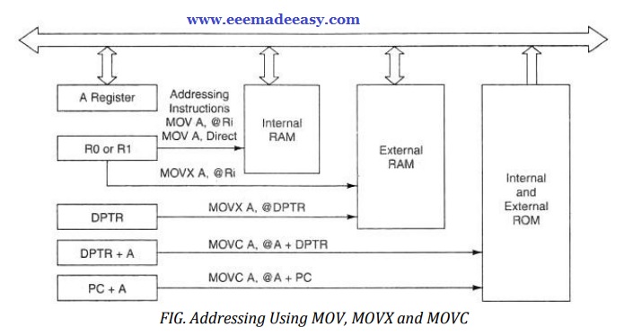
g. Move the contents of an external memory to A or A to an external memory
i. MOVX A,@R1
ii. MOVX @R0,A
iii. MOVX A,@DPTR
iv. MOVX@DPTR,A
h. Move the contents of program memory to A
i. MOVC A, @A+PC
ii. MOVC A, @A+DPTR
i. Push and Pop instructions
[SP]=07 //CONTENT OF SP IS 07 (DEFAULT VALUE)
MOV R6, #25H [R6]=25H //CONTENT OF R6 IS 25H
MOV R1, #12H [R1]=12H //CONTENT OF R1 IS 12H
MOV R4, #0F3H [R4]=F3H //CONTENT OF R4 IS F3H
PUSH 6 [SP]=08 [08]=[06]=25H //CONTENT OF 08 IS 25H
PUSH 1 [SP]=09 [09]=[01]=12H //CONTENT OF 09 IS 12H
PUSH 4 [SP]=0A [0A]=[04]=F3H //CONTENT OF 0A IS F3H
POP 6 [06]=[0A]=F3H [SP]=09 //CONTENT OF 06 IS F3H
POP 1 [01]=[09]=12H [SP]=08 //CONTENT OF 01 IS 12H
POP 4 [04]=[08]=25H [SP]=07 //CONTENT OF 04 IS 25H
j. Exchange instructions
The content of source ie., register, direct memory or indirect memory will be exchanged
with the contents of destination ie., accumulator.
i. XCH A,R3
ii. XCH A,@R1
iii. XCH A,54h
k. Exchange digit.
Exchange the lower order nibble of Accumulator (A0-A3) with lower
order nibble of the internal RAM location which is indirectly addressed by the register.
i. XCHD A,@R1
ii. XCHD A,@R0
Arithmetic instructions
The 8051 can perform addition, subtraction. Multiplication and division operations on 8 bit
numbers.
Addition
In this group, we have instructions to
i. Add the contents of A with immediate data with or without carry.
i. ADD A, #45H
ii. ADDC A, #OB4H
ii. Add the contents of A with register Rn with or without carry.
i. ADD A, R5
ii. ADDC A, R2
iii. Add the contents of A with contents of memory with or without carry using direct and
indirect addressing
i. ADD A, 51H
ii. ADDC A, 75H
iii. ADD A, @R1
iv. ADDC A, @R0
CY AC and OV flags will be affected by this operation.
Subtraction
In this group, we have instructions to
i. Subtract the contents of A with immediate data with or without carry.
i. SUBB A, #45H
ii. SUBB A, #OB4H
ii. Subtract the contents of A with register Rn with or without carry.
i. SUBB A, R5
ii. SUBB A, R2
iii. Subtract the contents of A with contents of memory with or without carry using direct and
indirect addressing
i. SUBB A, 51H
ii. SUBB A, 75H
iii. SUBB A, @R1
iv. SUBB A, @R0
CY AC and OV flags will be affected by this operation.
Multiplication
MUL AB.
This instruction multiplies two 8-bit unsigned numbers which are stored in the A and B
registers.
After multiplication, the lower byte of the result will be stored in the accumulator and higher
byte of result will be stored in the B register.
Eg. MOV A,#45H ;[A]=45H
MOV B,#0F5H ;[B]=F5H
MUL AB ;[A] x [B] = 45 x F5 = 4209 ;[A]=09H, [B]=42H
Division
DIV AB.
This instruction divides the 8-bit unsigned number which is stored in A by the 8-bit
the unsigned number which is stored in the B register.
After division, the result will be stored in the accumulator and the remainder will be stored in the B register.
Eg. MOV A,#45H ;[A]=0E8H
MOV B,#0F5H ;[B]=1BH
DIV AB ;[A] / [B] = E8 /1B = 08 H with remainder 10H ;[A] = 08H, [B]=10H
DA A (Decimal Adjust After Addition).
When two BCD numbers are added, the answer is a non-BCD number.
To get the result in BCD, we use DA A instruction after the addition. DA A works as follows.
If lower nibble is greater than 9 or auxiliary carry is 1, 6 is added to lower nibble.
If upper nibble is greater than 9 or carry is 1, 6 is added to upper nibble.
Eg 1: MOV A,#23H
MOV R1,#55H
ADD A,R1 // [A]=78
DA A // [A]=78 no changes in the accumulator after DA A
Eg 2: MOV A,#53H
MOV R1,#58H
ADD A,R1 // [A]=ABh
DA A // [A]=11, C=1 .
THE ANSWER IS 111. Accumulator data is changed after DA A
Increment: increments the operand by one.
INC A , INC Rn , INC DIRECT, INC @R ,iINC DPTR
INC increments the value of the source by 1. If the initial value of the register is FFH, incrementing the value will cause it to reset to 0.
The Carry Flag is not set when the value “rolls over” from 255 to 0.
In the case of “INC DPTR”, the value two-byte unsigned integer value of DPTR is incremented.
If the initial value of DPTR is FFFFh, incrementing the value will cause it to reset to 0.
Decrement:
decrements the operand by one.
DEC A DEC Rn DEC DIRECT DEC @Ri
DEC decrements the value of the source by 1. If the initial value of is 0, decrementing the value will cause it to reset to FFh.
The Carry Flag is not set when the value “rolls over” from 0 to FFh.
Logical Instructions
Logical AND
ANL destination, source:
ANL does a bitwise “AND” operation between the source and destination,
leaving the resulting value in the destination.
The value in source is not affected. “AND” instruction logically AND the bits of source and destination.
ANL A,#DATA ANL A, Rn
ANL A,DIRECT ANL A,@Ri
ANL DIRECT,A ANL DIRECT, #DATA
Logical OR
ORL destination, source: ORL does a bitwise “OR” operation between source and destination,
leaving the resulting value in destination.
The value in source is not affected. ” OR ” instruction logically OR the bits of source and destination.
ORL A,#DATA ORL A, Rn
ORL A,DIRECT ORL A,@Ri
ORL DIRECT,A ORL DIRECT, #DATA
Logical Ex-OR
XRL destination, source: XRL does a bitwise “EX-OR” operation between source and destination, leaving the resulting value in destination.
The value in source is not affected. ” XRL ” instruction logically EX-OR the bits of source and destination.
XRL A,#DATA XRL A,Rn
XRL A,DIRECT XRL A,@Ri
XRL DIRECT,A XRL DIRECT, #DATA
Logical NOT
CPL complements operand, leaving the result in operand.
If operand is a single bit then the state of the bit will be reversed. If operand is the Accumulator then all the bits in the Accumulator will be reversed.
CPL A, CPL C, CPL bit address
SWAP A – Swap the upper nibble and lower nibble of A.
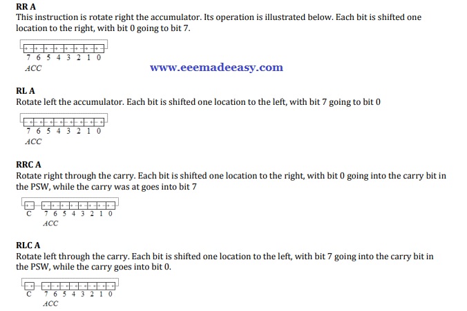
Rotate Instructions
RR A
This instruction is rotate right the accumulator. Its operation is illustrated below. Each bit is shifted one location to the right, with bit 0 going to bit 7.
Branch (JUMP) Instructions
Jump and Call Program Range
There are 3 types of jump instructions. They are:-
Relative Jump
Short Absolute Jump
Long Absolute Jump
Relative Jump
Jump that replaces the PC (program counter) content with a new address that is greater than (the
address following the jump instruction by 127 or less) or less than (the address following the jump
by 128 or less) is called a relative jump. Schematically, the relative jump can be shown as follows:
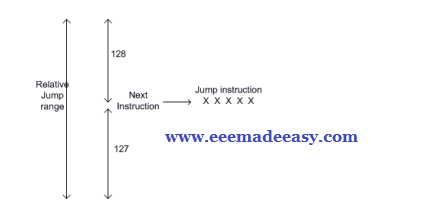
1. Only 1 byte of jump address needs to be specified in the 2’s complement form, ie. For jumping ahead, the range is 0 to 127 and for jumping back, the range is -1 to -128.
2. Specifying only one byte reduces the size of the instruction and speeds up program execution.
3. The program with relative jumps can be relocated without reassembling to generate absolute jump addresses.
Disadvantages of the absolute jump
1. Short jump range (-128 to 127 from the instruction following the jump instruction) Instructions that use Relative Jump SJMP ; this is unconditional jump
The remaining relative jumps are conditional jumps JC JNC JB bit, JNB bit, JBC bit, CJNE , , DJNZ , JZ JNZ Short Absolute Jump In this case only 11bits of the absolute jump address are needed. The absolute jump address is calculated in the following manner.
In 8051, 64 kbyte of program memory space is divided into 32 pages of 2 kbyte each.
The hexadecimal addresses of the pages are given as follows:-
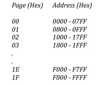
It can be seen that the upper 5bits of the program counter (PC) hold the page number and the lower 11bits of the PC hold the address within that page.
Thus, an absolute address is formed by taking page numbers of the instruction (from the program counter) following the jump and attaching the specified 11bits to it to form the 16-bit address.
Advantage: The instruction length becomes 2 bytes.
Example of short absolute jump: – ACALL AJMP
Long Absolute Jump/Call
Applications that need to access the entire program memory from 0000H to FFFFH use long absolute jump.
Since the absolute address has to be specified in the op-code, the instruction length is 3 bytes (except for JMP @ A+DPTR). This jump is not re-locatable.
Example: – LCALL LJMP JMP @A+DPTR Another classification of jump instructions is
1. Unconditional Jump
2. Conditional Jump
1. The unconditional jump is a jump in which control is transferred unconditionally to the target location.
a. LJMP (long jump).
This is a 3-byte instruction.
First byte is the op-code and second and third bytes represent the 16-bit target address which is any memory location from 0000 to FFFFH
eg: LJMP 3000H
b. AJMP:
this causes unconditional branch to the indicated address, by loading the 11 bit address to 0 -10 bits of the program counter.
The destination must be therefore within the same 2K blocks. c. SJMP (short jump). This is a 2-byte instruction.
First byte is the op-code and second byte is the relative target address, 00 to FFH (forward +127 and backward -128 bytes from the current PC value).
To calculate the target address of a short jump, the second byte is added to the PC value which is address of the instruction immediately below the jump.
Conditional Jump instructions
JBC Jump if bit = 1 and clear bit
JNB Jump if bit = 0
JB Jump if bit = 1
JNC Jump if CY = 0
JC Jump if CY = 1
CJNE reg,#data Jump if byte ≠ #data
CJNE A,byte Jump if A ≠ byte
DJNZ Decrement and Jump if A ≠ 0
JNZ Jump if A ≠ 0
JZ Jump if A = 0
All conditional jumps are short jumps.
Bit level jump instructions:
Bit level JUMP instructions will check the conditions of the bit and if condition is true, it jumps to the address specified in the instruction.
All the bit jumps are relative jumps.
JB bit, rel ; jump if the direct bit is set to the relative address specified.
JNB bit, rel ; jump if the direct bit is clear to the relative address specified.
JBC bit, rel ; jump if the direct bit is set to the relative address specified and then clear the bit.
Subroutine CALL And RETURN Instructions
Subroutines are handled by CALL and RET instructions
There are two types of CALL instructions
- LCALL address(16 bit)
This is long call instruction which unconditionally calls the subroutine located at the indicated 16 bit
address. This is a 3 byte instruction. The LCALL instruction works as follows.
a. During execution of LCALL, [PC] = [PC]+3; (if address where LCALL resides is say, 0x3254;
during execution of this instruction [PC] = 3254h + 3h = 3257h
b. [SP]=[SP]+1; (if SP contains default value 07, then SP increments and [SP]=08
c. [[SP]] = [PC7-0]; (lower byte of PC content ie., 57 will be stored in memory location 08.
d. [SP]=[SP]+1; (SP increments again and [SP]=09)
e. [[SP]] = [PC15-8]; (higher byte of PC content ie., 32 will be stored in memory location 09.
With these the address (0x3254) which was in PC is stored in stack.
f. [PC]= address (16 bit);the new address of subroutine is loaded to PC. No flags are affected. - ACALL address(11 bit)
This is absolute call instruction which unconditionally calls the subroutine located at the indicated 11 bit address. This is a 2 byte instruction. The SCALL instruction works as follows.
a. During execution of SCALL, [PC] = [PC]+2; (if address where LCALL resides is say, 0x8549;
during execution of this instruction [PC] = 8549h + 2h = 854Bh
b. [SP]=[SP]+1; (if SP contains default value 07, then SP increments and [SP]=08
c. [[SP]] = [PC7-0]; (lower byte of PC content ie., 4B will be stored in memory location 08.
d. [SP]=[SP]+1; (SP increments again and [SP]=09)
e. [[SP]] = [PC15-8]; (higher byte of PC content ie., 85 will be stored in memory location 09.
With these the address (0x854B) which was in PC is stored in stack.
f. [PC10-0]= address (11 bit); the new address of subroutine is loaded to PC. No flags are
affected.
RET instruction
RET instruction pops top two contents from the stack and load it to PC.
g. [PC15-8] = [[SP]] ;content of current top of the stack will be moved to higher byte of PC.
h. [SP]=[SP]-1; (SP decrements)
i. [PC7-0] = [[SP]] ;content of bottom of the stack will be moved to lower byte of PC.
j. [SP]=[SP]-1; (SP decrements again)
Bit manipulation instructions.
8051 has 128 bit addressable memory. Bit addressable SFRs and bit addressable PORT pins.
It is possible to perform following bit wise operations for these bit addressable locations.
- LOGICAL AND
a. ANL C,BIT(BIT ADDRESS) ; ‘LOGICALLY AND’ CARRY AND CONTENT OF BIT ADDRESS, STORE RESULT IN CARRY
b. ANL C, /BIT; ; ‘LOGICALLY AND’ CARRY AND COMPLEMENT OF CONTENT OF BIT ADDRESS, STORE RESULT IN CARRY - LOGICAL OR
a. ORL C,BIT(BIT ADDRESS) ; ‘LOGICALLY OR’ CARRY AND CONTENT OF BIT ADDRESS, STORE RESULT IN CARRY
b. ORL C, /BIT; ; ‘LOGICALLY OR’ CARRY AND COMPLEMENT OF CONTENT OF BIT ADDRESS, STORE RESULT IN CARRY - CLR bit
a. CLR bit ; CONTENT OF BIT ADDRESS SPECIFIED WILL BE CLEARED.
b. CLR C ; CONTENT OF CARRY WILL BE CLEARED. - CPL bit
a. CPL bit ; CONTENT OF BIT ADDRESS SPECIFIED WILL BE COMPLEMENTED.
b. CPL C ; CONTENT OF CARRY WILL BE COMPLEMENTED.
Books for Microcontroller 8051
- KSEB Sub Engineer and AE Books
- The 8051 Micro controller 3rd Edition,by Kenneth Ayala
- The 8051 Microcontrollers & Embedded Systems, by Mazidi
- 8051 MICROCONTROLLER AND APPLICATIONS FOR BSC
- Microcontroller & Embedded Systems for BE
Read More on Microcontrollers
- Features of AVR|AVR Microcontrollers
- 8051 ARCHITECTURE|8051 Microcontroller Architecture
- 8051 Microcontroller Architecture|RISC and CISC CPU Architectures|HARVARD & VON- NEUMANN CPU Architecture
- Microprocessor VS Microcontroller| Comparison of Microprocessor and Microcontroller|Difference between Microprocessor and Microcontroller
- Addressing modes of 8051 Microcontroller|8051 Addressing Modes
- 8051 Microcontroller Instruction Set|KSEB Sub Engineer Notes
- 8051 Microcontroller MCQ|8051 Questions and Answers
- Microcontroller|Types of microcontroller
- 8051 Microcontroller Notes pdf|8051 microcontroller pdf
- Interrupts in 8051|Interrupts in 8051 Microcontroller
- [New] AE KWA Kerala PSC 2026
- [New] Electricity Worker KSEB Syllabus 2026|021/2026 Syllabus Kerala PSC
- [Latest]KWA Operator Syllabus 2026|734,735/2025 Kerala PSC syllabus
- [New]Inspector of Legal Metrology Syllabus|613/2025 Kerala PSC Syllabus
- [PDF]IE Rules|Indian Electricity Rules 1956

- [Latest]Syllabus Sub Engineer LSGD Electricity Wing Thrissur Corporation| 770/2025 Syllabus Kerala PSC
- Compensating Windings
- Transformers Electrical Engineering Interview Questions
- DC Motor Electrical Engineering Interview Questions
- Special Electrical Machines Interview Questions
- 125 Electrical Engineering Interview Questions
- Syllabus Training Instructor Plumber|14/2025 Syllabus Kerala PSC