8051 Architecture: In this post, the Block diagram of the 8051 Microcontroller is explained. Learn more about each block in 8051 Architecture.
8051 Microcontroller Architecture
Salient features of 8051 microcontroller
- Eight bit CPU
- On-chip clock oscillator
- 4Kbytes of internal program memory (code memory) [ROM]
- 128 bytes of internal data memory [RAM]
- 64 Kbytes of external program memory address space.
- 64 Kbytes of external data memory address space.
- 32 bi directional I/O lines (can be used as four 8 bit ports or 32 individually addressable I/O lines)
Read more: Microcontroller|Types of microcontroller
- Two 16 Bit Timer/Counter :T0, T1
- Full Duplex serial data receiver/transmitter
- Four Register banks with 8 registers in each bank.
- Sixteen bit Program counter (PC) and a data pointer (DPTR)
- 8 Bit Program Status Word (PSW)
- 8 Bit Stack Pointer
- Five vector interrupt structure (RESET not considered as an interrupt.)
- 8051 CPU consists of 8 bit ALU with associated registers like accumulator ‘A’ , B register, PSW, SP, 16 bit program counter, stack pointer.
- ALU can perform arithmetic and logic functions on 8 bit variables.
- 8051 has 128 bytes of internal RAM which is divided into
- Working registers [00 – 1F]
- Bit addressable memory area [20 – 2F]
- General purpose memory area (Scratch pad memory) [30-7F]
Download & Install EEE Made Easy App
for more reference
- Microcontroller Architecture|RISC and CISC CPU Architectures|HARVARD & VON- NEUMANN CPU Architecture
- 8051 Microcontroller MCQ|8051 Questions and Answers
- Program|Machine language|object code|Assembly language|source code
Join EEE Made Easy Telegram channel
8051 Microcontroller Architecture -Block Diagram
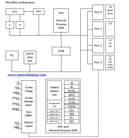
8051 has 4 K Bytes of internal ROM. The address space is from 0000 to 0FFFh. If the program size is more than 4 K Bytes 8051 will fetch the code automatically from external memory.
Accumulator
The accumulator is an 8 bit register widely used for all arithmetic and logical operations. Accumulator is also used to transfer data between external memory.
B register is used along with Accumulator for multiplication and division.
A and B registers together is also called MATH registers.
PSW (Program Status Word)
This is an 8 bit register which contains the arithmetic status of ALU and the bank select bits of register banks.
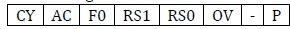
CY – carry flag
AC – auxiliary carry flag
F0 – available to the user for general purpose
RS1,RS0 – register bank select bits
OV – overflow
P – parity
Stack Pointer (SP)
Stack Pointer (SP) – it contains the address of the data item on the top of the stack. Stack may reside anywhere on the internal RAM. On reset, SP is initialized to 07 so that the default stack will start from address 08 onwards.
Data Pointer (DPTR)
Data Pointer (DPTR) – DPH (Data pointer higher byte), DPL (Data pointer lower byte). This is a 16 bit register which is used to furnish address information for internal and external program memory and for external data memory.
Program Counter (PC)
Program Counter (PC) – 16 bit PC contains the address of next instruction to be executed. On reset PC will set to 0000. After fetching every instruction PC will increment by one.
8051 PIN DIAGRAM
8051 PIN diagram consists of 40 pins. Each PIN function is detailed below.
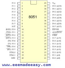
8051 Pinout Description
Pins 1-8: PORT 1. Each of these pins can be configured as an input or an output.
Pin 9: RESET. A logic one on this pin disables the microcontroller and clears the contents of most registers.
In other words, the positive voltage on this pin resets the microcontroller.
By applying logic zero to this pin, the program starts execution from the beginning.
Pins10-17 PORT 3. Similar to port 1, each of these pins can serve as general input or output. Besides, all of them have alternative functions
Pin 10 RXD. Serial asynchronous communication input or Serial synchronous communication output.
Pin 11 TXD. Serial asynchronous communication output or Serial synchronous communication clock output.
Pin 12 INT0.External Interrupt 0 input
Pin 13 INT1. External Interrupt 1 input
Pin 14 T0. Counter 0 clock input
Pin 15 T1. Counter 1 clock input
Pin 16 WR. Write to external (additional) RAM
Pin 17 RD. Read from external RAM
Pin 18, 19 XTAL2, XTAL1. Internal oscillator input and output. A quartz crystal which specifies operating frequency is usually connected to these pins.
Pin 20 GND. Ground.
Pin 21-28 Port 2. If there is no intention to use external memory then these port pins are configured as general inputs/outputs. In case external memory is used, the higher address byte, i.e. addresses A8-A15 will appear on this port. Even though memory with capacity of 64Kb is not used, which means that not all eight port bits are used for its addressing, the rest of them are not available as inputs/outputs.
Pin 29 PSEN. If external ROM is used for storing program then a logic zero (0) appears on it every time the microcontroller reads a byte from memory.
Pin 30 ALE. Prior to reading from external memory, the microcontroller puts the lower address byte (A0-A7) on P0 and activates the ALE output.
After receiving signal from the ALE pin, the external latch latches the state of P0 and uses it as a memory chip address.
Immediately after that, the ALE pin is returned its previous logic state and P0 is now used as a Data Bus.
Pin 31 EA. By applying logic zero to this pin, P2 and P3 are used for data and address transmission with no regard to whether there is internal memory or not.
It means that even there is a program written to the microcontroller, it will not be executed. Instead, the program written to external ROM will be executed.
By applying logic one to the EA pin, the microcontroller will use both memories, first internal then external (if exists).
Pin 32-39 PORT 0. Similar to P2, if external memory is not used, these pins can be used as general inputs/outputs.
Otherwise, P0 is configured as address output (A0-A7) when the ALE pin is driven high (1) or as data output (Data Bus) when the ALE pin is driven low (0).
Pin 40 VCC. +5V power supply.
8051 Memory Organization
8051 Memory organization consists of Internal RAM, registers, Bit addressable RAM, General purposr RAM and Stack.
Internal RAM organization
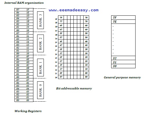
Register Banks:
00h to 1Fh: The 8051 uses 8 general-purpose registers R0 through R7 (R0, R1, R2, R3, R4, R5, R6, and R7).
There are four such register banks. Selection of register bank can be done through RS1,RS0 bits of PSW. On reset, the default Register Bank 0 will be selected.
Bit Addressable RAM:
20h to 2Fh. The 8051 supports a special feature which allows access to bit variables.
This is where individual memory bits in Internal RAM can be set or cleared.
In all there are 128 bits numbered 00h to 7Fh.
Being bit variables any one variable can have a value 0 or 1.
A bit variable can be set with a command such as SETB and cleared with a command such as CLR.
Example instructions are:
SETB 25h ; sets the bit 25h (becomes 1)
CLR 25h ; clears bit 25h (becomes 0) Note, bit 25h is actually bit 5 of Internal RAM location 24h.
The Bit Addressable area of the RAM is just 16 bytes of Internal RAM located between 20h and 2Fh.
General Purpose RAM:
30h to 7Fh. Even if 80 bytes of Internal RAM memory are available for general-purpose data storage, user should take care while using the memory location from 00 -2Fh
since these locations are also the default register space, stack space, and bit addressable space.
It is a good practice to use general-purpose memory from 30 – 7Fh. The general purpose RAM can be accessed using direct or indirect addressing modes
STACK
A stack is a last-in-first-out memory.
In 8051 internal RAM space can be used as stack.
The address of the stack is contained in a register called stack pointer. Instructions PUSH and POP are used for stack operations.
When a data is to be placed on the stack, the stack pointer increments before storing the data on the stack so that the stack grows up as data is stored (pre-increment).
As the data is retrieved from the stack the byte is read from the stack, and then SP decrements to point the next available byte of stored data (post decrement).
The stack pointer is set to 07 when the 8051 resets.
So that default stack memory starts from address location 08 onwards (to avoid overwriting the default register bank ie., bank 0).
Eg; Show the stack and SP for the following.
[SP]=07 //CONTENT OF SP IS 07 (DEFAULT VALUE)
MOV R6, #25H [R6]=25H //CONTENT OF R6 IS 25H
MOV R1, #12H [R1]=12H //CONTENT OF R1 IS 12H
MOV R4, #0F3H [R4]=F3H //CONTENT OF R4 IS F3H
PUSH 6 [SP]=08 [08]=[06]=25H //CONTENT OF 08 IS 25H
PUSH 1 [SP]=09 [09]=[01]=12H //CONTENT OF 09 IS 12H
PUSH 4 [SP]=0A [0A]=[04]=F3H //CONTENT OF 0A IS F3H
POP 6 [06]=[0A]=F3H [SP]=09 //CONTENT OF 06 IS F3H
POP 1 [01]=[09]=12H [SP]=08 //CONTENT OF 01 IS 12H
POP 4 [04]=[08]=25H [SP]=07 //CONTENT OF 04 IS 25H
Read more on 8051 Microcontroller
- Addressing modes of 8051 Microcontroller|8051 Addressing Modes
- Microprocessor VS Microcontroller| Comparison of Microprocessor and Microcontroller|Difference between Microprocessor and Microcontroller
- 8051 Microcontroller Instruction Set|KSEB Sub Engineer Notes
- Industrial Automation Introduction|Sub Engineer KSEB Industrial Automation
- POWER DIODE TYPES
- [Latest]Sub Engineer Electrical KSEB Detailed Syllabus Download PDF| KSEB Sub Engineer Syllabus
Books for Microcontroller 8051
- KSEB Sub Engineer and AE Books
- The 8051 Micro controller 3rd Edition,by Kenneth Ayala
- The 8051 Microcontrollers & Embedded Systems, by Mazidi
- 8051 MICROCONTROLLER AND APPLICATIONS FOR BSC
- Microcontroller & Embedded Systems for BE
- Compensating Windings

- Transformers Electrical Engineering Interview Questions
- DC Motor Electrical Engineering Interview Questions
- Special Electrical Machines Interview Questions
- 125 Electrical Engineering Interview Questions
- Syllabus Training Instructor Plumber|14/2025 Syllabus Kerala PSC
- [PDF] Syllabus AE KSEB Transfer|378/2025 Syllabus Kerala PSC
- Modified Harvard Architecture
- TMS320C5X Architecture
- Advantages of Digital Signal Processing
- [PDF] AE Agro Industries Corporation syllabus|595/2024 syllabus Kerala PSC
- Tellengen’s Theorem & Example