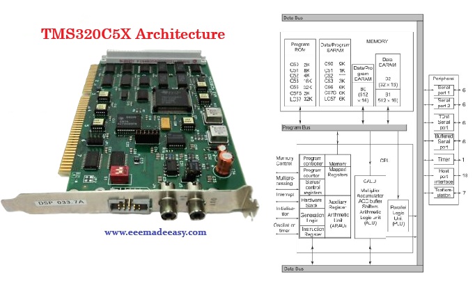
TMS320C5X Architecture:The TMS320 DSP family consists of two types of single-chip DSPs: 16-bit fixed-point and 32-bit floating-point. These DSPs possess the operational flexibility of high-speed controllers and the numerical capability of array processors.
Combining these two qualities, the TMS320 processors are inexpensive alternatives to custom fabricated VLSI and multichip bit-slice processors.
TMS320C5X DSP family
TMS320C5X belongs to the fi fth generation of the TI’s TMS320 family of DSPs. The first fi ve generations of TMS320 family are
C1X, C2X, C3X, C4X and C5X. The C1X, C2X, C2XX and C5X are 16-bit fixed-point processors.
Instruction sets of the higher generation fi xed-point processors are upward compatible to the lower
generation fixed-point processors. For example C5X can execute the instructions of both C1X and C2X.
The 54X is upward compatible with 5X. C3X and C4X are 32-bit fl oating-point processors and C4X
is upward compatible with C3X instruction set.
The sixth generation C6X devices feature VelociTI™, an advanced very long instruction word (VLIW) architecture developed by TI and can execute 1600
MIPS. The eighth-generation C8X devices, have, on a single piece of silicon, a number of advanced
DSPs (ADSPs) and a RISC master processor. Typical application of the above families of TI DSPs are
as follows:
C1X, C2X, C2XX, C5X, C54X: toys, hard disk drives, modems, cellular phones and active car
suspensions
C3X: fi lters, analysers, hi-fi systems, voice mail, imaging, bar-code readers, motor control, 3D
graphics or scientifi c processing
C4X: parallel-processing clusters in virtual reality, image recognition telecom routing, and parallelprocessing
systems.
C6X: wireless base stations, pooled modems, remote-access servers, digital subscriber loop systems,
cable modems and multichannel telephone systems
C8X: video telephony, 3D computer graphics, virtual reality and a number of multimedia applications
The TI DSP chips have IC numbers with the prefi x TMS320. If the next letter is C (e.g. TMS320C5X),
it indicates that CMOS technology is used for the IC and the on-chip non-volatile memory is a ROM.
If it is E (e.g. TMS320E5X) it indicates that the technology used is CMOS and the on-chip non-volatile
memory is an EPROM.
If it is neither (e.g. TMS3205X), it indicates that NMOS technology is used
for the IC and the on-chip non-volatile memory is a ROM. Under C5X itself there are three processors,
‘C50, ‘C51 and ‘C5X, that have identical instruction set but have differences in the capacity of on-chip
ROM and RAM. The characteristics of some of the TMS320 family DSP chips are given in Table 3.1.
The instruction set of TMS320C5X and other DSP chips is superior to the instruction set of
conventional microprocessors such as 8085, Z80, etc., as most of the instructions require only a single
cycle for execution. The multiply accumulate operation used quite frequently in signal processing
applications such as convolution requires only one cycle in DSP.
Characteristics of some of the TMS320 family DSP chips

Architecture of TMS320C5X DSPs
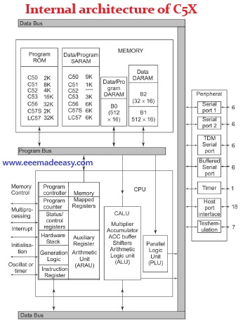
The block diagram of the internal architecture of C5X is shown in Fig. . The 320C5X DSPs are said to have advanced Harvard architecture because they have separate memory bus structures for program and data and have instructions that enable data transfer between the program and data memory area.
SOME FLAGS IN THE STATUS REGISTERS
The status registers can be stored into data memory and loaded from data memory, thereby allowing the
‘C5X status to be saved and restored for subroutines. The ST0 and ST1 each have an associated 1-level
deep shadow register stack for automatic context-saving when an interrupt trap is taken. These registers
are automatically restored upon a return from interrupt.
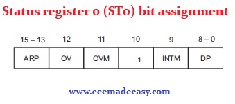
The bit assignment details for ST0 and ST1 are given in Fig. Signifi cance of the various bits of
ST0 and ST1 are as follows:
ARP (Auxiliary Register Pointer) These bits select the AR to be used in indirect addressing. When the
ARP is loaded, the previous ARP value is copied to the auxiliary register buffer (ARB) in ST1.
OV (Overfl ow) fl ag bit This bit indicates that an arithmetic operation overfl ow in the ALU.
OVM (Overfl ow Mode) bit This bit enables/disables the accumulator overfl ow saturation mode in the
ALU.
INTM (Interrupt Mode) bit This bit globally masks or enables all interrupts. The INTM bit has no effect
on the non-maskable R
—
S
–
and N
—
M
—
I interrupts.
DP (Data Memory Page Pointer) bits These bits specify the address of the current data memory page.
The DP bits are concatenated with the 7 LSBs of an instruction word to form a direct memory address
of 16 bits.
Characteristics of some of the TMS320 family DSP chips
Separate program and data buses allow simultaneous access to program instructions and data, providing
a high degree of parallelism. For example, while data is multiplied, a previous product can be loaded
into, added to or subtracted from the accumulator and, at the same time, a new address can be generated.
Such parallelism supports a powerful set of arithmetic, logic and bit-manipulation operations that can
all be performed in a single machine cycle. In addition, the ¢C5X includes the control mechanisms to
manage interrupts, repeated operations and function calling. The ¢C5X architecture has four buses and
their functions are as follows:
Program bus (PB) It carries the instruction code and immediate operands from program memory
space to the CPU.
Program address bus (PAB) It provides addresses to program memory space for both reads and
writes.
Data read bus (DB) It interconnects various elements of the CPU to data memory space.
Data read address bus (DAB) It provides the address to access the data memory space. The program
and data buses can work together to transfer data from on-chip data memory and internal or external
program memory to the multiplier for single-cycle multiply/accumulate operations.
CPU registers (except STO and ST1), peripheral registers and I/O ports occupy data memory space.
Some of the registers/execution units in the CPU of C5X DSP processors and their functions are as
follows.
CENTRAL ARITHMETIC LOGIC UNIT (CALU)
It consists of the following elements: (16xl6)-bit parallel multiplier, arithmetic logic unit (ALU),
accumulator (ACC), accumulator buffer (ACCB), product register (PREG) each with 32 bits and 0-16-
bit left barrel shifter and right barrel shifter.
One of the operands for the ALU operation comes from ACC. The result of operations performed in
central ALU are stored in ACC. Either the higher order word or lower order word of ACC can be loaded
from memory. A 32-bit register denoted as ACCB is used for temporary storage of ACC. The hardware
multiplier unit in the C5X processors performs 16 x 16 multiplication of numbers represented in 2’s
complement form. The 32-bit PREG holds the result of multiplication. The 16-bit temporary register 0
(TREG0) holds the multiplicand. The other operand for the multiplication can be specifi ed using one of
the addressing modes.
0-16-bit left barrel shifter and right barrel shifter in CALU permit the contents of memory to be
left shifted by 0 to 16 bits before they are either fed to ALU or stored from ALU to memory. The CPU
registers ACC and PREG can also be shifted using these shifters. In this case they require two cycles.
A 5-bit register TREG1 specifi es the number of bits by which the scaling shifter should shift either the
incoming data to one of the CPU registers or vice versa. When the incoming data to CPU is left shifted
by the scaling shifter the LSBs are fi lled with 0.
AUXILIARY REGISTER ALU (ARAU)
It consists of eight 16-bit auxiliary registers (ARs) AR0-AR7, a 3-bit auxiliary register pointer (ARP)
and an unsigned 16-bit ALU. ARAU calculates indirect addresses by using inputs from ARs, 16-bit index
register (INDX) and auxiliary register compare register (ARCR). The ARAU can autoindex the current
AR while the data memory location is being addressed and can index either by ± 1 or by the contents of
the INDX. As a result, accessing data does not require the CALU for address manipulation; therefore,
the CALU is free for other operations in parallel. This makes the instructions to be executed faster
compared to the conventional microprocessors. For example, let us consider the following sequence of
8085 instructions:
M0V A,M
INX H
These instructions enable the accumulator to be loaded using indirect addressing mode and HL
register used as the address pointer is incremented. These two instructions can be replaced by a single
5X instruction LACC *+, 0.
Further, any one of the auxiliary registers can be used as the address pointer and incremented by the
above instruction. The register that will be used is specifi ed by the content of the ARP.
The auxiliary registers AR0-AR7 may also be used as the general purpose registers for holding the
operands for arithmetic and logical operations in CALU. Some of the other registers of ARAU and their
functions are as follows:
INDEX REGISTER (INDX)
The 16-bit INDX is used by the ARAU as a step value (addition or subtraction by more than 1) to
modify the address in the ARs during indirect addressing. For example, when the ARAU steps across
a row of a matrix, the indirect address is incremented by 1. However, when the ARAU steps down a
column, the address is incremented by the dimension of the matrix. The ARAU can add or subtract the
value stored in the INDX from the current AR as part of the indirect address operation. INDX can also
map the dimension of the address block used for bit-reversal addressing.
AUXILIARY REGISTER COMPARE REGISTER (ARCR)
The 16-bit ARCR is used for address boundary comparison. The CMPR instruction compares the ARCR
to the selected AR and places the result of the compare in the TC bit of ST1.
BLOCK MOVE ADDRESS REGISTER (BMAR)
The 16-bit BMAR holds an address value to be used with block moves and multiply/accumulate
operations. This register provides the 16-bit address for an indirect-addressed second operand.
BLOCK REPEAT REGISTERS (RPTC, BRCR, PASR, PAER)
All these registers are 16-bit wide. Repeat counter register (RPTC) holds the repeat count in a repeat
single-instruction operation and is loaded by the RPT and RPTZ instructions. Block repeat counter
register (BRCR) holds the count value for the block repeat feature. This value is loaded before a block
repeat operation is initiated. Block repeat program address start register (PASR) indicates the 16-bit
address where the repeated block of code starts. The block repeat program address end register (PAER)
indicates the 16-bit address where the repeated block of code ends. The PASR and PAER are loaded by
the RPTB instruction.
PARALLEL LOGIC UNIT (PLU)
It performs Boolean operations or the bit manipulations required of high-speed controllers. The PLU
can set, clear, test or toggle bits in a status register control register, or any data memory location. The
PLU allows logic operations to be performed on data memory values directly without affecting the
contents of the ACC or PREG. Results of a PLU function are written back to the original data memory
location.
MEMORY-MAPPED REGISTERS
The ‘C5X has 96 registers mapped into page 0 of the data memory space. All ‘C5X DSPs have 28 CPU
registers and 16 input/output (I/O) port registers but have different numbers of peripheral and reserved
registers. Since the memory-mapped registers are a component of the data memory space, they can be
written to and read from in the same way as any other data memory location. The memory-mapped
registers are used for indirect data address pointers, temporary storage, CPU status and control, or
integer arithmetic processing through the ARAU.
PROGRAM CONTROLLER
The program controller contains logic circuitry that decodes the instructions, manages the CPU pipeline,
stores the status of CPU operations and decodes the conditional operations. Parallelism of architecture lets
the ¢C5X perform three concurrent memory operations in any given machine cycle: fetch an instruction,
read an operand and write an operand. The program controller consists of the following elements:
16-bit program counter (PC)
16-bit status registers ST0, ST1, processor mode status register (PMST) and circular buffer control
register (CBCR)
(8 x 16)-bit hardware stack
Address generation logic
Instruction register
Interrupt fl ag register and interrupt mask register
Status register 0 (ST0) bit assignment
Fig. 3.2(b) Status register 1 (ST1) bit assignment
ARB Auxiliary Register Buffer
This 3-bit fi eld holds the previous value contained in the ARP in ST0. Whenever the ARP is loaded, the
previous ARP value is copied to the ARB, except when using the LST #0 instruction. When the ARB
is loaded using the LST #1 instruction, the same value is also copied to the ARP. This is useful when
restoring context (when not using the automatic context save) in a subroutine that modifi es the current
ARP.
CNF On-chip RAM confi guration control bit This 1-bit fi eld enables the on-chip dual-access RAM
block 0 (DARAM B0) to be addressable in data memory space or program memory space. The CNF bit
can be modifi ed by the LST #1 instruction. If CNF is 0, the on-chip DARAM block 0 is mapped into
data memory space. The CNF bit can be cleared by a reset or the CLRC CNF instruction. When CNF is
1, the on-chip DARAM block 0 is mapped into program memory space. The CNF bit can be set by the
SETC CNF instruction.
TC Test/control fl ag bit This 1-bit fl ag stores the results of the ALU or parallel logic unit (PLU) test
bit operations. The status of the TC bit determines if the conditional branch, call and return instructions
are to be executed.
SXM Sign-extension mode bit This 1-bit fi eld enables/disables sign extension of an arithmetic operation.
The SXM bit does not affect the operations of certain arithmetic or logical instructions; the ADDC,
ADDS, SUBB or SUBS instruction suppresses sign extension, regardless of SXM.
C Carry bit This 1-bit fi eld indicates an arithmetic operation carry or borrow in the ALU. The singlebit
shift and rotate instructions affect the C bit.
HM Hold mode bit This 1-bit fi eld determines whether the central processing unit (CPU) stops or
continues execution when acknowledging an active H
—
OL —
D —
signal.
XF pin status bit This 1-bit fi eld determines the level of the external fl ag (XF) output pin.
PM Product shift mode bits This 2-bit fi eld determines the product shifter (P-SCALER) mode and
shift value for the PREG output into the ALU. Table 3.2 gives the PM bits and the function performed.
PM bits and the function performed
PM bits Function
b1 b0 P-SCALER mode for PREG output
0 0 No shift
0 1 Left-shifted 1 bit; LSB zero-fi lled
1 0 Left-shifted 4 bits; 4 LSBs zero-fi lled
1 1 Right-shifted 6 bits; sign extended; 6 LSBs lost. The product is always sign extended, regardless
of the value of the SXM bit
ON-CHIP MEMORY
The ¢C5X architecture contains a considerable amount of on-chip memory to aid in system performance
and integration:
Program Read-Only Memory (ROM)
Data/Program Dual-Access RAM (DARAM)
Data/Program Single-Access RAM (SARAM)
The ¢C5X has a total address range of 224K words x 16 bits. The memory space is divided into
four individually selectable memory segments: 64K-word program memory space, 64K-word local data
memory space, 64K-word I/O ports and 32K-word global data memory space.
Program ROM
All ‘C5X DSPs carry a 16-bit on-chip maskable programmable ROM (see Fig. 3.1 for sizes). Some of
the ‘C5X DSPs have boot loader code resident in the on-chip ROM, and the other ¢C5X DSPs offer
the boot loader code as an option. This memory is used for booting program code from slower external
ROM or EPROM to fast on-chip or external RAM. Once the custom program has been booted into
RAM, the boot ROM space can be removed from program memory space by setting the MP/ MC bit
in the processor mode status register (PMST). The on-chip ROM is selected at reset by driving the
MP/ MC pin low. If the on-chip ROM is not selected, the ‘C5X devices start execution from off-chip
memory.
Data/Program Dual-Access RAM
All ¢C5X DSPs carry a 1056-word x 16-bit on-chip dual-access RAM (DARAM). The DARAM is
divided into three individually selectable memory blocks: 512-word data or program DARAM block
B0, 512-word data DARAM block B1 and 32-word data DARAM block B2. The DARAM is primarily
intended to store data values but, when needed, can be used to store programs as well. DARAM blocks
B1 and B2 are always confi gured as data memory; however. DARAM block B0 can be confi gured by
software as data or program memory.
DARAM improves the operational speed of the ‘C5X CPU. The CPU operates with a 4-deep pipeline.
In this pipeline, the CPU reads data on the third stage and writes data on the fourth stage. Hence, for
a given instruction sequence, the second instruction could be reading data at the same time the fi rst
instruction is writing data. The dual data buses (DB and DAB) allow the CPU to read from and write to
DARAM in the same machine cycle.
Data/Program Single-Access RAM
Almost all ¢C5X DSPs carry a 16-bit on-chip single-access RAM (SARAM) of sizes varying from
1-9K (16–bits) words. Code can be booted from an off-chip ROM and then executed at full speed once
it is loaded into the on-chip SARAM. The SARAM can be confi gured by software as data memory, as
program memory or combination of both data memory and program memory. The SARAM is divided
into 1K- and/or 2K-word blocks contiguous in address memory space. All ¢C5X CPUs support parallel
accesses to these SARAM blocks. However, one SARAM block can be accessed only once per machine
cycle. In other words, the CPU can read from or write to one SARAM block while accessing another
SARAM block.
On-Chip Memory Protection
The C5X DSPs have a maskable option that protects the contents of on-chip memories. When the
related bit is set, no externally originating instruction can access the on-chip memory spaces.
ON-CHIP PERIPHERALS
All ¢C5X DSPs have the same CPU structure; however, they have different on-chip peripherals connected
to their CPUs. The ‘C5X DSP on-chip peripherals available are as follows:
Clock Generator
Hardware Timer
Software-Programmable Wait-State Generators
Parallel I/O Ports
Host Port Interface (HPI)
Serial Port
Buffered Serial Port (BSP)
Time-Division Multiplexed (TDM) Serial Port
User-Maskable Interrupts
Clock Generator
The clock generator consists of an internal oscillator and a phaselocked loop (PLL) circuit. The clock
generator can be driven internally by a crystal resonator circuit or driven externally by a clock source.
The PLL circuit can generate an internal CPU clock by multiplying the clock source by a specifi c factor
and so a clock source with a frequency lower than that of the CPU can be used.
Hardware Timer
A 16-bit hardware timer with a 4-bit prescaler is available. This programmable timer clocks at a rate
that is between 1/2 and 1/32 of the machine cycle rate (CLKOUT1), depending upon the timer’s dividedown
ratio. The timer can be stopped, restarted, reset or disabled by specifi c status bits. Three registers
control and operate the timer. The timer counter register (TIM) gives the current count of the timer. The
timer period register (PRD) defi nes the period for the timer. The 16-bit timer control register (TCR)
controls the operations of the timer.
Software-Programmable Wait-State Generators
Software-programmable wait-state logic is incorporated in ‘C5X DSPs allowing wait-state generation
without any external hardware for interfacing with slower off-chip memory and I/O devices. This
feature consists of multiple wait-state generating circuits. Each circuit is user-programmable to operate
in different wait states for off-chip memory accesses.
Parallel I/O Ports
A total of 64K I/O ports are available, 16 of these ports are memory-mapped in data memory space.
Each of the I/O ports can be addressed by the IN or the OUT instruction. The memory-mapped I/O ports
can be accessed with any instruction that reads from or writes to data memory. The IS signal indicates
a read or write operation through an I/O port. The ¢C5X can easily interface with external I/O devices
through the I/O ports while requiring minimal off-chip address decoding circuits.
Host Port Interface (HPI)
The HPI is available on the ¢C57S and ¢LC57. It is an 8-bit parallel I/O port that provides an interface
to a host processor. Information is exchanged between the DSP and the host processor through on-chip
memory that is accessible to both the host processor and the ‘C57.
Serial Port
Three different kinds of serial ports are available: a general-purpose serial port, a time-division
multiplexed (TDM) serial port and a buffered serial port (BSP). Each ¢C5X contains at least one generalpurpose,
high-speed synchronous, full-duplexed serial port interface that provides direct communication
with serial devices such as codecs, serial analog-to-digital (A/D) converters and other serial systems.
The serial port is capable of operating at up to one-fourth the machine cycle rate (CLKOUT1). The
serial port transmitter and receiver are double-buffered and individually controlled by maskable external
interrupt signals. Data is framed either as bytes or as words.
Five 16-bit registers (SPC, DRR, DXR, XSR, RSR) control and operate the serial port interface. The
serial port control (SPC) register contains the mode control and status bits of the serial port. The data
receive register (DRR) holds the incoming serial data, and the data transmit register (DXR) holds the
outgoing serial data. The data transmit shift register (XSR) controls the shifting of the data from the
DXR to the output pin. The data receive shift register (RSR) controls the storing of the data from the
input pin to the DRR.
Buffered Serial Port (BSP)
The BSP is available on the ¢C56 and ¢C57 devices. It is a full-duplexed, double-buffered serial port and
an autobuffering unit (ABU). The BSP provides fl exibility on the data stream length. The ABU supports
high-speed data transfer and reduces interrupt latencies. The BSP has a 2K-word buffer, which resides
in the ‘C5X internal memory. Five BSP registers control and operate the BSP.
TDM Serial Port
The TDM serial port available on the ‘C50, ‘C51 and ‘C53 devices is a full-duplexed serial port that can
be confi gured by software either for synchronous operations or for time-division multiplexed operations.
The TDM serial port is commonly used in multiprocessor applications.
User-Maskable Interrupts
Four external interrupt lines (IN —
T
—
1 – IN
—
T
—
4) and fi ve internal interrupts, a timer interrupt and four serial
port interrupts are user maskable. When an interrupt service routine (ISR) is executed, the contents
of the program counter are saved on an 8-level hardware stack, and the contents of 11 specifi c CPU
registers, ACC, ACCB, PREG, ST0, ST1, PMST, TREG0, TREG1, TREG2, INDX and ARCR, are
saved in one deep stack (shadow registers). When a return from interrupt instruction is executed, the
CPU registers’ contents are restored.